Tampilkan postingan dengan label Semiconductor. Tampilkan semua postingan

Measurement of the Higgs boson mass and width using the four-lepton final state in proton-proton collisions at √s = 13 TeV

 Measurement-of-the-Higgs-boson-mass-and-width-using-the-four-lepton-final-state-in-proton-proton-collisions-10


A measurement of the Higgs boson mass and width via its decay to two Z bosons is presented. Proton-proton collision data collected by the CMS experiment, corresponding to an integrated luminosity of 138 fb^−1 at a center-of-mass energy of 13 TeV, is used. The invariant mass distribution of four leptons in the on-shell Higgs boson decay is used to measure its mass and constrain its width. This yields the most precise single measurement of the Higgs boson mass to date, 125.04 ± 0.12 GeV, and an upper limit on the width Γ H < 330 MeV at 95% confidence level. A combination of the on-and off-shell Higgs boson production decaying to four leptons is used to determine the Higgs boson width, assuming that no new virtual particles affect the production, a premise that is tested by adding new heavy particles in the gluon fusion loop model. This result is combined with a previous CMS analysis of the off-shell Higgs boson production with decay to two leptons and two neutrinos, giving a measured Higgs boson width of 3.0 +2.0, −1.5 MeV, in agreement with the standard model prediction of 4.1 MeV. The strength of the off-shell Higgs boson production is also reported. The scenario of no off-shell Higgs boson production is excluded at a confidence level corresponding to 3.8 standard deviations.


Higgs boson mass and width measurements with on-shell production

The Higgs boson mass and width are measured, using on-shell production, by fitting the m4â„“ distribution in the mass range 105 < m4â„“ < 140 GeV. The results have been determined using the CMS statistical analysis tool COMBINE, which is based on the ROOFIT and ROOSTATS frameworks. Table 1 shows the mass measurements obtained from the 1D approach, where no further assumptions have been made. In comparison to the 1D model, the 1D′BS model reduces the uncertainty by about 15%. Implementing the δm4â„“/m4â„“ categorization then gives the N –1D′BS model, which leads to an additional 10% improvement. Finally, using the D kin, bkg discriminant to reduce the background produces the N –2D′BS model with another 4% improvement. Table 5 shows the resulting m4â„“ measurements using this last model. All the measured m4â„“ values from the different fits are statistically compatible, given their uncertainties and correlations. Figure 1 displays the observed 1D likelihood scans as functions of mH, from the fits for the different 4â„“ categories and combined. Combining all the m4â„“ final states and data-taking years, our final result is mH = 125.04 ± 0.11 (stat) ± 0.05 (syst) = 125.04 ± 0.12 GeV. The largest systematic uncertainty is from the lepton momentum scale and equals 0.03 and 0.04 GeV for final states with muons and electrons, respectively. 

Table 1: Best fit values for the mass of the Higgs boson measured in the inclusive 4â„“ final state and separately for different flavor categories using the 1D approach. Uncertainties are separated into statistical and systematic uncertainties. Expected uncertainties are also given assuming mH = 125.38 GeV 

Measurement-of-the-Higgs-boson-mass-and-width-using-the-four-lepton-final-state-in-proton-proton-collisions-1

Table 2: Best fit values for the mass of the Higgs boson measured in the inclusive 4â„“ final state and separately for different flavor categories, using the final fit configuration (N –2D’BS). Uncertainties are separated into statistical and systematic uncertainties. Expected uncertainties are also given assuming mH = 125.38 GeV.

Measurement-of-the-Higgs-boson-mass-and-width-using-the-four-lepton-final-state-in-proton-proton-collisions-2


As a check on the analysis technique and the systematic uncertainty from this method, the 1D′BS model is applied to Z → 4â„“ events in the m4â„“ range 70–105 GeV. The signal shape is obtained using a convolution of a Breit–Wigner function and a double-sided Crystal Ball function. The fitted values of mZ in different subchannels are m4µ Z = 91.02 ± 0.14 GeV, m4e Z = 91.18 ± 0.45 GeV, m2e2µ Z = 91.40 ± 0.29 GeV, and m2e2µ Z = 91.40 ± 0.37 GeV, leading to a combined value of mZ = 91.17 ± 0.12 GeV, consistent with the world-average Z boson mass and with the uncertainty in agreement with the expected value of ± 0.12 GeV from simulation. The results from this analysis are combined with those extracted using data recorded with the CMS detector during Run 1 at √ s = 7 and 8 TeV. Since this analysis uses an improved method to extract the systematic uncertainties affecting lepton momentum, the lepton energy scales and resolution uncertainties are considered uncorrelated between the two runs. The combined observed result from both data-taking periods is mH = 125.08 ± 0.12 GeV = 125.08 ± 0.10 (stat)±0.05 (syst) GeV. The corresponding expected statistical and systematic uncertainties are ±0.10 and ±0.05 GeV, respectively. Figure 2 presents a summary of the Higgs boson mass measurements by the CMS Collaboration in the four-lepton decay channel.


Measurement-of-the-Higgs-boson-mass-and-width-using-the-four-lepton-final-state-in-proton-proton-collisions-3

Figure 1: The profile likelihood from the mH fit using the N –2D′BS model for each of the 4â„“ categories and combined. The change in likelihood corresponding to 68 and 95% CLs are shown by the dashed horizontal lines. Both statistical and systematic uncertainties are included in the fits.


Measurement-of-the-Higgs-boson-mass-and-width-using-the-four-lepton-final-state-in-proton-proton-collisions-4

Figure 2: Summary of the CMS Higgs boson mass measurements using the four-lepton final state. The red vertical line and the gray column represent the best fit value and the total uncertainty, respectively, as measured by combining the Runs 1 and 2 data. The yellow band and horizontal black bars show the statistical and total uncertainties in each measurement, respectively. The value of each measurement is given, along with the total and statistical only (in parentheses) uncertainties.


 Higgs boson width measurement with off-shell production

Table 3: Summary of the total Higgs boson width ΓH measurement, showing the 68% CL (central values with uncertainties) and 95% CL (in square brackets) intervals for the H → ZZ → 4â„“ channel alone and in combination with the off-shell H → ZZ → 2â„“2ν channel.

Measurement-of-the-Higgs-boson-mass-and-width-using-the-four-lepton-final-state-in-proton-proton-collisions-5

Measurement-of-the-Higgs-boson-mass-and-width-using-the-four-lepton-final-state-in-proton-proton-collisions-6
Figure 3: Observed (solid) and expected (dashed) profile likelihood projections from the Higgs boson width fit using on- and off-shell production from this analysis. The analysis of the offshell H → ZZ → 4â„“ channel combined with the on-shell H → ZZ → 4â„“ channel is shown in black. The full combination of H → ZZ → 4â„“ with the off-shell H → ZZ → 2â„“2ν is given in red. The black horizontal dashed lines show the 68 and 95% CL values. 


The observed limits on Î“H are stronger than the average expected values from simulation. This is supported by the upper left, where the number of observed events in the sensitive region of m4â„“ > 340 GeV and Dbkg > 0.6 in the Untagged category is below the expected value, but still consistent with it. The smaller number of events in this region favors the hypothesis of negative interference between the signal and background contributions, which dominates over the pure signal contributions for Î“H values near the SM value. Therefore, large and very small values of ΓH are disfavored. 


A measurement of the Higgs boson mass (mH) and width (ΓH) using the decays to two Z bosons is presented. The data sample comes from proton-proton collisions at the LHC recorded by the CMS experiment at a center-of-mass energy of 13 TeV, corresponding to an integrated luminosity of 138 fb−1 . On-shell Higgs boson production with the H → 4â„“ decay (â„“ = e, µ) is used to measure its mass and constrain its width. The mass measurement yields mH = 125.04± 25.

 Table 4: Measured values of the signal strengths µ off-shell , µ off-shell, F , and µ off-shell, V , and their 68% and 95% (in square brackets) CL intervals from the combined fit to the off-shell H → ZZ → 4â„“ and 2â„“2ν channels.

Measurement-of-the-Higgs-boson-mass-and-width-using-the-four-lepton-final-state-in-proton-proton-collisions-7


Measurement-of-the-Higgs-boson-mass-and-width-using-the-four-lepton-final-state-in-proton-proton-collisions-8
Figure 4: Observed 2D profile likelihood projection of the off-shell signal strength parameters (µ off-shell, F , and Âµ off-shell, V  ) from the fit to the combined off-shell H → ZZ → 4â„“ and 2â„“2ν channels. The best fit value is shown by the black cross and the SM prediction by the red x. The 68 and 95% CL contours are given by the dashed and solid curves, respectively. The color scale to the right of the plot relates the quantitative values. 


0.11 (stat) ± 0.05 (syst) GeV = 125.04 ± 0.12 GeV, in agreement with the expected precision of ±0.12 GeV. From on-shell production events, an upper limit of Î“H < 330 MeV is set at 95% confidence level. The mass measurement is further improved by combining data from Runs 1 and 2, leading to the most precise single measurement of the mass to date in this channel, mH = 125.08 ± 0.10 (stat) ± 0.05 (syst) GeV = 125.08 ± 0.12 GeV. Using on- and off-shell Higgs boson production with the decay to four leptons, and combining them with a separate analysis with Higgs boson decay to two leptons plus two neutrinos, we measure Î“H = 3.0+2.0, −1.5 MeV, consistent with the standard model prediction of 4.1 MeV. These results are summarized in Table 5. The strength of the off-shell Higgs boson production is also reported, and the scenario of no off-shell Higgs boson production is excluded at a confidence level corresponding to 3.8 standard deviations. Results of the measurements are tabulated in the HEPData record for this analysis.


Table 5: Summary of the Higgs boson mass and total width Î“H measurements, showing the allowed 68% CL (central values with uncertainties) and 95% CL (in square brackets) intervals. Uncertainties are reported as a combination of statistical and systematic uncertainties. The first two rows display the outcomes of the analysis conducted within the on-shell H → ZZ → 4â„“ region, where the width is restricted to be positive. The third row incorporates results from the off-shell H → ZZ → 4â„“ region combined with the on-shell H → ZZ → 4â„“ and off-shell H → ZZ → 2â„“2ν.

Measurement-of-the-Higgs-boson-mass-and-width-using-the-four-lepton-final-state-in-proton-proton-collisions-9

                                                       ====== Physics =======


Read more:

Ultrafast Switch from a Bose-Einstein Condensate Matter - Practicalintroduction

A Theoretical Perspective : Spin−Orbit Coupling in 2D Semiconductors

Bill Gates Reveals Technology That Will Dethrone Smartphones, What The Technology Is?

Neuromorphic Spintronics - Neuromorphic Computing with Spin Torque Nano-oscillators

Cellular Lasers for Cell Imaging and Biosensing


References :

S. L. Glashow, “Partial-symmetries of weak interactions”, Nucl. Phys. 22 (1961) 579, doi:10.1016/0029-5582(61)90469-2. 

F. Englert and R. Brout, “Broken symmetry and the mass of gauge vector mesons”, Phys. Rev. Lett. 13 (1964) 321, doi:10.1103/PhysRevLett.13.321. 

CMS Collaboration, “The CMS statistical analysis and combination tool: COMBINE”, Comput. Softw. Big Sci. 8 (2024) 19, doi:10.1007/s41781-024-00121-4, arXiv:2404.06614. 

W. Verkerke and D. P. Kirkby, “The RooFit toolkit for data modeling”, in Proceedings of the 13th International Conference for Computing in High-Energy and Nuclear Physics (CHEP03). 2003. arXiv:physics/0306116. 

L. Moneta et al., “The RooStats project”, PoS ACAT2010 (2010) 057, doi:10.22323/1.093.0057, arXiv:1009.1003. 

CMS Collaboration, “A measurement of the Higgs boson mass in the diphoton decay channel”, Phys. Lett. B 805 (2020) 135425, doi:10.1016/j.physletb.2020.135425, arXiv:2002.06398. 

Particle Data Group, K. A. Olive et al., “Review of Particle Physics”, Chin. Phys. C 38 (2014) 090001, doi:10.1088/1674-1137/38/9/090001. 

CMS Collaboration, “Measurement of the properties of a Higgs boson in the four-lepton final state”, Phys. Rev. D 89 (2014) 092007, doi:10.1103/PhysRevD.89.092007, arXiv:1312.5353.

“HEPData record for this analysis”, 2024. doi:10.17182/hepdata.153670.


Share:

Neuromorphic Spintronics - Neuromorphic Computing with Spin Torque Nano-oscillators


Neuromorphic-Spintronics-Neuromorphic-Computing-with-Spin-Torque-Nano-oscillators-1

Neuromorphic computing uses basic principles inspired by the brain to design circuits that perform artificial intelligence tasks with superior energy efficiency. Traditional approaches have been limited by the energy area of artificial neurons and synapses realized with conventional electronic devices.

In recent years, multiple groups have demonstrated that spintronic nanodevices, which exploit the magnetic as well as electrical properties of electrons, can increase the energy efficiency and decrease the area of these circuits. Among the variety of spintronic devices that have been used, magnetic tunnel junctions play a prominent role because of their established compatibility with standard integrated circuits and their multifunctionality.

Magnetic tunnel junctions can serve as synapses, storing connection weights, functioning as local, nonvolatile digital memory or as continuously varying resistances. As nano-oscillators, they can serve as neurons, emulating the oscillatory behavior of sets of biological neurons. As superparamagnets, they can do so by emulating the random spiking of biological neurons. Magnetic textures like domain walls or skyrmions can be configured to function as neurons through their non-linear dynamics.

Several implementations of neuromorphic computing with spintronic devices demonstrate their promise in this context. Used as variable resistance synapses, magnetic tunnel junctions perform pattern recognition in an associative memory. As oscillators, they perform spoken digit recognition in reservoir computing and when coupled together, classification of signals. As superparamagnets, they perform population coding and probabilistic computing.

Simulations demonstrate that arrays of nanomagnets and films of skyrmions can operate as components of neuromorphic computers. While these examples show the unique promise of spintronics in this field, there are several challenges to scaling up, including the efficiency of coupling between devices and the relatively low ratio of maximum to minimum resistances in the individual devices.


Neuromorphic-Spintronics-Neuromorphic-Computing-with-Spin-Torque-Nano-oscillators-2

figure 1.

(a) Magnetic tunnel junctions for memory applications. A magnetic junction consists of two ferromagnetic layers (gray) separated by an insulating layer (blue) with the magnetization of one layer fixed and that of the other either parallel (low resistance) or antiparallel (high resistance) to it.

(b) Cross-bar array of magnetic tunnel junctions for high density storage (Magnetic Random Access Memory). The resistance of a particular tunnel junction is measured by activating the appropriate word line (red) allowing conduction between the bottom bit line and the top sense line (both blue). The alignment of the magnetization can be switched by passing sufficient currents through the device.

(c) Associative memory. (i) Handwritten digits from the MNIST dataset used for training the associative memory. (ii) Sample test input after training. (iii) Output of trained network from the test input showing successful association.


Neuromorphic-Spintronics-Neuromorphic-Computing-with-Spin-Torque-Nano-oscillators-3

Figure 2. Neuromorphic computing with Spin Torque nano-oscillators. 

(a) Schematic spin torque nano-oscillator. When designed appropriately, the free layer magnetization of a tunnel junction precesses when a dc current is passed through it. Because of the oscillating magnetoresistance, a fixed input current gives an oscillating voltage across the junction. 

(b) Reservoir computing with a spin torque nano-oscillator. Using time multiplexing in pre- and post-processing, a single spin torque nano-oscillator gives state of the art performance as a reservoir in a reservoir computing scheme. 

(c) Schematic use of coupled nano-oscillators for vowel recognition. The input is represented by the frequencies of two microwaves applied through a stripline to the oscillators. The natural frequencies of the oscillators are tuned by dc bias currents through the devise. These can be tuned so that the synchronization pattern between the oscillators corresponds to the desired output.

Neuromorphic-Spintronics-Neuromorphic-Computing-with-Spin-Torque-Nano-oscillators-4

Figure 3

(a) Schematic skyrmion structure. The magnetization direction of a single skyrmion is schematically given both by the directions of the arrows and the color coding, ranging from blue for magnetization up, through white for in-plane magnetization directions, to red for magnetization down. (b) Simulated skyrmion assembly. A reservoir computing scheme based on skyrmions in a random potential makes use of the distortions of the assembly due to current flow to provide the necessary non-linearity and memory.


Read more:

Ultrafast Switch from a Bose-Einstein Condensate Matter - Practicalintroduction

A Theoretical Perspective : Spin−Orbit Coupling in 2D Semiconductors

Bill Gates Reveals Technology That Will Dethrone Smartphones, What The Technology Is?

Measurement of the Higgs boson mass and width using the four-lepton final state in proton-proton collisions at √s = 13 TeV

Cellular Lasers for Cell Imaging and Biosensing


References :

1. Big data needs a hardware revolution. Nature (2018). doi:10.1038/d41586-018-01683-1 

2. Furber S Large-scale neuromorphic computing systems. J. Neural Eng 13, 051001 (2016). [PubMed: 27529195] 

3. Indiveri G et al. Neuromorphic silicon neuron circuits. Neuromorphic Eng 5, 73 (2011). 

4. Locatelli N, Cros V & Grollier J Spin-torque building blocks. Nat. Mater 13, 11–20 (2014). [PubMed: 24343514] 

5. Grollier J, Querlioz D & Stiles MD Spintronic Nanodevices for Bioinspired Computing. Proc. IEEE 104, 2024–2039 (2016).


Share:

Ultrafast Switch from a Bose-Einstein Condensate Matter - Practicalintroduction

reviewed by: Indrawan Vpp

A subpicosecond optical switch demonstrated in a semiconductor material moves researchers a step closer to an all-optical computer.

Ultrafast-Switch-from-a-Bose-Einstein-Condensate1


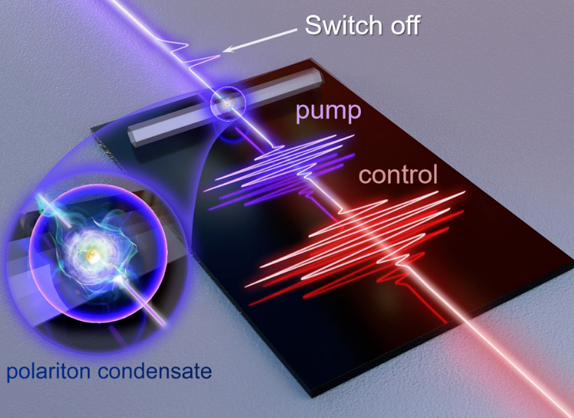
When “pumped” with an ultraviolet laser pulse, the microwire (light gray strip) acts as a microcavity containing quasiparticles called exciton polaritons that form a Bose-Einstein condensate (BEC). A red “control” pulse a few picoseconds later causes the BEC’s emitted light (purple beam, upper left) to shut off in less than a picosecond (sharp drop after first output pulse) before recovering moments later (wider output pulse). The “off” signal corresponds to the gap between the two output pulses. 


Light-based information-processing chips could provide a huge improvement in processing power and speed over today’s electronics, but one of the challenges to their development is creating optically-controlled switches that are fast. A new trick for allowing one light signal to control another in a semiconducting material now pushes switching times from around a picosecond (10−12 seconds) to as much as 100 times faster in a device that can be readily integrated onto a chip [1]. The rapid switching is achieved by exploiting a Bose-Einstein condensate (BEC)—a quantum state famous for exotic behavior in superconductors and cold gases—in a new way. The work paves the way to extremely high-frequency optical information technologies.


Optoelectronic switching—using light to control a current—has previously been demonstrated within just 1 femtosecond (10−12 seconds) but only in a semiconductor device that is difficult to fabricate and to operate [2]. A different approach to making chip-based optical devices exploits electronic excitations called exciton polaritons, formed when a photon trapped in an optical cavity interacts with an electronic state called an exciton (a combination of an electron and a “hole,” or absence of an electron). The photon and exciton can bind into a quasiparticle, the exciton polariton.

Exciton polaritons can interact with light in ways that change abruptly as the intensity of the light is changed. In particular, an optical pulse can cause the light emitted by these quasiparticles to decline abruptly to zero intensity. Polariton-based optical switches have been reported previously with switching times of a picosecond or so [3, 4].


A team in China led by Hui Li of East China Normal University wanted to speed up switching by using a BEC of polaritons, where the quasiparticles “condense” into a single quantum state. Bose-Einstein condensation generally happens only at ultralow temperatures, but exciton polaritons in semiconductor microcavities can form a BEC even at room temperature [5]. Such polariton condensates have been used before in optical switches and other devices [3, 6], but Li and colleagues suspected that they could achieve much faster switching with a new technique. They wanted to exploit the way a “control” pulse of light can interact with the photon part of the quasiparticles to rapidly clear many of the polaritons out of the BEC state and abruptly switch the system off.


The team’s polariton BEC is formed in a microcavity—a zinc oxide wire, 3.6 micrometers in cross-section—from exciton polaritons created by an ultraviolet pump pulse that lasts only a few femtoseconds. The pump photons bounce around within the wire’s hexagonal cross-section and interact with excitons in the material to form polaritons. The polaritons condense into a BEC of around 20 million quasiparticles that decays within a few picoseconds. The pump pulse serves as the input signal; while the BEC lasts, some of its photons are emitted and can be detected as the output.


The control pulse from a red laser disrupts the condensate, depleting it of polaritons and switching off the output signal. Li says that this disruption happens in less than a picosecond—about 100 times faster than earlier polariton switches. What is more, the ratio of on-to-off signal (extinction ratio) in the device is about a million—the best achieved in a polariton switch. The researchers say that the switching speed might be sped up by 10 times by shortening the duration of the control pulse.


“This is very nice work, and I’m impressed by their results,” says quantum optics expert Daniel Suárez Forero of the University of Maryland in College Park. “It is nice to see how, 27 years after the first experimental demonstration of a BEC, the control of systems hosting this phenomenon has improved to the point that technological applications can be implemented.”


He praises the room temperature operation, fast switching times, and high extinction ratio of the device. Such properties “make these systems very suitable for ultrafast switching technologies,” he says. But Suárez Forero cautions that there are still important challenges to overcome—for example, miniaturizing all the components of the setup, including the lasers.


References :

A. Schiffrin et al., “Optical-field-induced current in dielectrics,” Nature 493, 70 (2012).

C. Antón et al., “Dynamics of a polariton condensate transistor switch,” Appl. Phys. Lett. 101, 261116 (2012).

J. Feng et al., “All-optical switching based on interacting exciton polaritons in self-assembled perovskite microwires,” Sci. Adv. 7 (2021).

Share:

Cellular Lasers for Cell Imaging and Biosensing - Review Practicalintroduction

Introduction


practicalintroduction.com


The availability of fluorescent dyes or molecules, such as organic fluorophores and naturally occurring luminescent proteins (e.g., green, yellow, and red fluorescent proteins), have advanced our understanding of molecular and cell biology through specific labeling of targets expressed in cells and tissues. This study advancement has been accompanied by developments in (confocal and super-resolution) fluorescence microscopy, (single-molecule) fluorescence spectroscopy, and flow cytometry. When fluorescent molecules are excited with an appropriate energy light source, there is the spontaneous emission of lower Energy Photon in a process known as fluorescence. These emitted photons possess broad emission wavelength characteristics (see representative simplified Jablonski diagram in Fig. 1a, 1c). 


As a very different approach, under certain circumstances, this spontaneous emission can be overcome by stimulated emission. Stimulated emission (Fig. 1b), coined for the first time by Albert Einstein in 1917, is an optical phenomenon in which an incoming photon of a specific wavelength interacts with the electron at the excited state, followed by relaxation to a lower ground energy level resulting in a new photon with identical phase, frequency, polarization, and direction of propagation as the photon source. This process is widely known as the foundation of light amplification in laser technology (i.e., laser stands for light amplification by stimulated emission of radiation). Depending on the type of gain medium, lasers are classified into different types (i.e., gas, solid-state, semiconductor, and organic lasers). In an organic laser setup, amplified stimulated emission can be obtained by optically pumping an active/gain medium (fluorescent dye), which is placed inside a well-defined optical cavity, typically a sandwich of highly reflective mirrors providing coherent optical feedback (Fig. 1d). 


Read more :


When the total gain inside the cavity is larger than the losses, the system reaches the threshold for lasing action to occur. The resulting laser emission is coherent and very narrow in terms of the spectrum in comparison to the fluorescence signal (Fig. 1c). A bio laser is a new class of organic lasers, defined as the integration of biomolecules or biomaterials in the laser system (Fig. 2). As with some (organic) fluorescent chromophores, certain materials (typically fluorescent biomolecules) can be used as the gain medium. Bio lasers have been achieved by placing green fluorescent proteins (GFP) or vitamins inside the optical cavity, e.g., Fabry-Pérot or distributed feedback (see Fig. 2a).


Biomaterials and biopolymers such as plant starch, egg white, polylactic acid, and poly(lactic-co-glycolic acid), which form natural spherical or ellipsoidal micro granules shapes, can also act as high-quality whispering-gallery-mode (WGM) resonators to provide sufficient optical gain for lasing. Another possible scenario is to use biomaterials, which are typically created as nano- and micro-structures serving as scatterers that can effectively provide optical feedback (i.e., in the case of random bio lasers, Fig. 2b). Non-fluorescent biomaterials can be further employed as interference/disturbance medium in the lasing systems (inside the cavity). In this regard, the alteration in lasing properties (i.e., increase of the optical losses due to unwanted scattering or refractive index difference) is expected, and it can reveal the optical properties of biomaterials. Organic micro/nanolasers have been significantly advanced over the last decade, especially related to the continuous improvement in controlling their lasing output. Different designs and controls of microcavities and organic optical gain media have been developed to build high-performance micro/nanolasers (i.e., wavelength-tunable lasers, multi-wavelength lasers, single-mode lasers, mode controllable lasers, and directional lasers). Among them, dual-wavelength single-mode lasing based on a mutual model selection mechanism was demonstrated in axially coupled organic heterogeneous nanowire resonators, in which each individual nanowire functions as both laser source and mode filter for the other nanowire. These nanowire resonators provided multiple nanoscale output ports to produce coherent signals with various colors increasing the integration level of such photonic devices. Besides, broadband tunable single-mode microlasers based on photoisomerization activated intramolecular charge-transfer process is coupled polymer microdisk cavities were also reported. 


In that review, the single-mode lasing could be reversibly tuned between ∼699 nm and ∼726 nm by alternating the UV and Vis irradiation. Host-guest composite organic microlasers have been further researched to reduce lasing thresholds, improve laser lifetime, and extend the tuning range. In such a configuration, the host materials do not only improve the lasing performances but also provide new functionalities for the organic microlasers, which it is expected can be more beneficial when used in real practical applications (e.g., toxic gas detection, biological sensing, and color laser display). For controlling the output of organic micro/nanolasers, current techniques are commonly based on external stimuli (i.e., light, force, heat, and vapor). However, in the case of practical applications (e.g., hybrid optoelectronic integration and interconnects), electrically controlled organic micro/nanolasers are more desirable.


Biological cells have recently emerged in the lasing system and have successfully been employed to generate laser action, which from this point onwards will be referred to as cellular lasers. In particular, cells or bacteria can be engineered to express certain fluorescent proteins. Unlike in a conventional fluorescence imaging setup, in which fluorescence signals are detected, once those entities have been placed inside an optical cavity, generation of stimulated emission upon sufficient optical pumping is very likely to occur (Fig. 2c). Cells exhibit different auto-fluorescence signals arising from endogenous molecules such as mitochondrial nicotinamide adenine dinucleotide (NADH) and flavin adenine dinucleotide (FAD), which can be used as an intrinsic photon source for light amplification. 


Moreover, the advances in the fields of cell staining and immunolabeling have allowed cells, including their cellular organelles (e.g., nuclei, lysosomes, endosomes, golgi complex, mitochondria, and cytoplasm) and cellular architectures (F-actins, microtubules, and intermediate filaments) to be specifically tagged with certain organic fluorophores or fluorescent-labeled antibodies. This opens the possibility to generate lasers from different sites within cells and more importantly, allows the production of cellular laser activity with more than single-wavelength laser radiation (i.e., multiplexing) upon multiple labeling. Lastly, the possibility to introduce fluorescent/luminescent particles (e.g., quantum dots, carbon dots, semiconductor nanowires, and fluorescently-labeled nanoparticles as gain media or probes into the cells can be also beneficial in developing cellular lasers.


Apart from placing a single cell or bacterium inside an optical cavity (or termed an external cavity), resonators can be also miniaturized and introduced inside the cell (i.e., internal cavity, Fig. 2d). The nature of the cells that tend to internalize objects of certain sizes (typically less than 1–2 µm) using a process called endocytosis will be important knowledge to deliver the cavity into the cytoplasmic region of the cells. In case the resonator is too large to be internalized naturally, transfection technology utilized for delivering DNA/RNA into the cells can be also opted. Once the cavity is present inside the cells, intracellular fluorescence coming from fluorescent proteins or organic fluorophores can be optically coupled to the cavity, and subsequently amplified.


In this review, all possible scenarios to generate cellular lasers are discussed. The potential applications of cellular lasers for next-generation cell imaging and cytometry as well as for cell analysis and distinction study are emphasized, while key remaining challenges in engineering the cellular lasers are highlighted. 


The possibility to produce laser action involving biomaterials, in particular (single) biological cells, has fostered the development of cellular lasers as a novel approach in biophotonics. In this respect, cells that are engineered to carry gain medium (e.g., fluorescent dyes or proteins) are placed inside an optical cavity (i.e., typically a sandwich of highly reflective mirrors), allowing the generation of stimulated emission upon sufficient optical pumping. In another scenario, micron-sized optical resonators supporting whispering-gallery-mode (WGM) or semiconductor-based laser probes can be internalized by the cells and support light amplification. This review summarizes the recent advances in the fields of bio lasers and cellular lasers, and most importantly, highlights their potential applications in the fields of in vitro and in vivo cell imaging and analysis. They include biosensing (e.g., in vitro detection of sodium chloride (NaCl) concentration), cancer cell imaging, laser-emission-based microscope, cell tracking, cell distinction study, and tissue contraction monitoring in zebrafish. 


Lastly, several fundamental issues in developing cellular lasers including laser probe fabrication, the biocompatibility of the system, and alteration of the local refractive index of optical cavities due to protein absorption or probe aggregation are described. Cellular lasers are foreseen as a promising tool to study numerous biological and biophysical phenomena.


Bio lasers are a generation of lasers involving biological materials. Biomaterials, including single cells, can be engineered to incorporate laser probes or fluorescent proteins, or fluorophores, and the resulting light emission can be coupled to an optical resonator, allowing the generation of cellular laser emission upon optical pumping. Unlike fluorescence, this stimulated emission is very sensitive and is capable of detecting small alterations in the optical property of the cells and their environment. 


In this review, recent development and applications of cellular lasers in the fields of in vitro and in vivo cell imaging, cell tracking, biosensing, and cell/tissue analysis are highlighted. Several challenges in developing cellular lasers including probe fabrication and biocompatibility as well as alteration of the cellular environment are explained.


Applications of cellular lasers


Promising applications of cellular lasers are in the fields of cell imaging, cell classification, biomechanical analysis, and biosensing. The generation of cellular lasers in general can give major advantages, such as improving the resolution and sensitivity of microscopic cell imaging. The intensity of laser emission possesses a multifold increase in the brightness compared to fluorescence emission, allowing the production of higher contrast images and overcoming the depth penetration issue during imaging of thick biological samples.


Generation of cellular lasers


practicalintroduction.com


One of the rising topics in the field of bio lasers nowadays is devoted to the involvement of biological organisms (e.g., single cells) in the lasing system. The general idea behind this is that single cells expressing fluorescent protein when placed inside an optical cavity, upon sufficient optical pumping, allow amplified stimulated emission to be generated.

Furthermore, Yun et al. and Gather et al. succeeded to extend the idea of cellular lasers by introducing the concept of lasers with both the gain medium and cavity being present inside cells

Recently, the integration and generation of inorganic intracellular lasers were demonstrated to have a WGM resonator with a size of < 1 µm. From that work, an intracellular laser with volumes 1000-fold smaller than the eukaryotic nucleus (Vlaser < 0.1 µm3) and lasing thresholds 500-fold below the pulse energies typically used in two-photon microscopy (Eth ≈ 0.13 pJ), as well as excellent spectral stability (<50 pm wavelength shift), was successfully achieved employing aluminum gallium phosphide (AlGaP) multi-quantum well nanodisks.

In addition to CdS nanowires and InGaAsP microdisks, gallium nitride (GaN) micro rods, which have normally been used by researchers as a building block for developing light-emitting diodes (LEDs) and field-effect transistors (FETs).


This review has highlighted the advancement of laser emission generation involving biological materials, including single cells. Different approaches and examples of cellular lasers, both with and without conventional optical cavities (e.g., Fabry–Pérot and whispering-gallery-mode (WGM)), have been described. In addition, unlike fluorescence which is less sensitive to the change in environments, the resulting laser possesses different properties (e.g., wavelength shifts) depending on the types and biological states of the cells, therefore opening a new possibility to be used for cell imaging and analysis. Moreover, several in vitro and in vivo biosensing applications (e.g., detection of salt concentration, cancer cell distinction (cytometry), and monitoring of cell mechanical properties) have been demonstrated using the developed cellular lasing technique.


Few challenges in designing the cellular laser experiment and laser probe including biocompatibility of the system and alteration of the local refractive index of optical cavities due to protein absorption or probe aggregation should be considered. The field of cellular laser has not been mature yet. However, this promising technology is expected to be further developed and employed to study many important biological and biophysical phenomena, in which the laser performance can be improved by its combination with nanotechnology (e.g., plasmonic enhancement by metallic nanoparticles), microfluidic, and deep learning approaches.


Future challenges and outlooks


Several aspects need to be considered while designing a cellular laser and its experiments, which include the following points:


While performing a cell seeding inside the cavity, the cell might not attach/adhere properly to the cavity wall due to its non-biocompatibility feature. This will lead to a change in cellular properties and in an extreme case can lead to cell death. Pre-functionalization of the cavity surface with a very thin layer of proteins (e.g., collagen or fibronectin) or biocompatible polymers (e.g., poly-l-lysine) can be employed as a strategy to improve cell adhesion.


The formation of abundant protein corona on the internal cavity can alter the refractive index of the cavity surface, therefore changing the lasing properties. The walls of the external cavity can technically adsorb abundant protein by means of electrostatic/van der Waals interaction. Polystyrene particles used as a WGM cavity have been demonstrated to adsorb certain types of proteins upon introduction to cell media. The use of serum-free medium or buffer (e.g., phosphate-buffered saline) is therefore suggested.


WGM resonators (e.g., polystyrene particles) and laser probes (e.g., fluorescent particles or semiconductor nanowires) can aggregate in cell media and inside the cell, which is not desired. Proper (chemical) surface functionalization is needed to make the probe colloidally stable.


Internalized WGM spheres or nanowires are likely to end up in the lysosomes, and digestive organelles of cells with very high acidity. In the long term, it can result in the destruction of the probes.


Biocompatibilities of the cavity, laser probe, and gain medium need to be considered while designing living cellular lasers. Therefore, the choice of materials should be planned accordingly. As an example, a very high concentration of fluorescent dyes has been shown to be toxic to cells.


Most cells naturally do not possess spherical geometry as they are adherent on the surface of culture plates. To produce spherical cells, proteolytic enzyme solutions (e.g., trypsin or accutase) can be beforehand used to detach the cell from the surface. Detached cells are normally round in shape.


Multiple labeling with different fluorophores targeting different organelles is possible, therefore providing an opportunity to produce multiple laser emissions from a single cell.


Fabrication of monodisperse microsphere bio lasers plays an important role to result in highly reproducible and stable WGM lasing performance. A microfluidic-based fabrication technique can be employed to generate monodisperse dye-doped protein microsphere bio lasers with a tunable size range of 50 – 150 µm. Meanwhile, obtaining an optofluidic ring resonator (OFRR) with the same size and wall thickness, and industrial fiber draw tower can be used to overcome reproducibility issues raised in lab-based low-cost fabrication techniques using CO2 laser pulling machines.


The bio-extracted materials utilized for bio lasers normally require complicated extraction and synthesis processes, which consequently suffer from high costs. Using a simple dehydration method or its modified process (microglassification™), low-cost microspheres made of various natural materials (e.g., goose egg white, bovine serum albumin (BSA), and chicken albumen) can be reproducibly created in different sizes.


Cavity with a high Q-factor and low threshold is highly desirable to minimize the biological damage of external pumping light and concentrated fluorophores to living cells and tissues. This will enhance the laser lifetime. It should be noted that efficient lasing emission only occurs above the lasing threshold.


The penetration of the commonly used lasers for excitation (e.g., UV – visible light (190 – 700 nm) and NIR‐I light (700 – 950 nm)) is limited to a depth of < 10 mm into the subcutaneous tissues. Further design and development of gain materials, which can be excited in the NIR‐II light region (1000 – 1700 nm), will contribute to deep tissue applications. The other feasible solutions are combining bio lasers with biocompatible optical waveguides that can transport light into deep tissues and using a two-photon imaging technique that provides less optical damage to cells and tissues.(Indrawan Vpp)

READ MORE ABOUT SCHOLARSHIPS:

New Information Scholarship Program 2022 at the University of Cambridge in UK

The Graduate Excellence Fellowships in University of Geneva 2022

Singapore Scholarship 2022 - SINGA


Share:

Full-zone Persistent Spin Textures with Giant Spin Splitting in Two-dimensional Group IV-V Compounds - Management Practicalintroduction

The study of relativistic effects in solids, i.e., the spin-orbit coupling (SOC), has attracted increasing interest in the field of spintronics since it allows for manipulation of electron’s spin degree of freedom without additional external magnetic field. Many intriguing SOCrelated phenomena were observed, including spin relaxation, spin Hall effect, spin galvanic effect, and spin ballistic transport. In a system lacking inversion symmetry, the SOC induces momentum (k)-dependent spin–orbit field (SOF), Ω( ~ ~k) ∝ E~ × ~p, where E~ is the electric field originated from the crystal inversion asymmetry and ~p is the momentum, that lifts Kramer’s spin degeneracy and leads to the nontrivial k-dependent spin textures of the spin-split bands through the so-called Rashba and Dresselhaus effects. In particular, the Rashba effect attracted much attention since it can be manipulated electrically to produce non-equilibrium spin polarization[9, 10], which plays an important role for spin-field effect transistors (SFET).

Practically, materials with strong Rashba effect are desirable in spintronic applications since a large Rashba SOC parameter is in favor of room temperature device operations. However, the strong Rashba SOC is also known to induce the undesired effect of causing spin decoherence, which plays a detrimental role for the spin lifetime. Due to the kdependent SOF, electron scatterings by defect and impurity randomize the spin in a diffusive transport regime, which induces the fast spin decoherence through the Dyakonov-Perel spin relaxation mechanism, and hence limits the performance of the spintronics functionality. This problem can further be resolved by designing the materials supporting unidirectional SOF. Under the unidirectional SOF, the spin textures are uniformly oriented in the k-space, resulting in the so-called persistent spin texture (PST), therefore enabling long-range spin transport without dissipation through persistent spin helix (PSH) mechanism.

Previously, GaAs/AlGaAs and InGaAs/InAlAs heterostructures have been reported to demonstrate the emergence of the PSH state arising from a balance between the strength of the Rashba and Dresselhaus SOCs; however, these artificial structures require atomic precision by tuning the quantum-well width and carefully controlled carrier densities through doping level and and applied external electric field.

Recently, a different method for achieving the PST has been proposed, implemented by enforcing the symmetry of the crystal. While it remains to be confirmed experimentally, this method allows us to design the PST without requiring the fine-tuning between the Rashba and Dresselhaus SOCs. For example, the PST was predicted in noncentrosymmetric materials having mirror symmetry (or glide mirror symmetry) operations as recently reported on bulk BiInO3, CsBiNb2O7, and several two-dimensional (2D) systems including WO2Cl2, GaXY (X=Se, Te; Y =Cl, Br, I) and various group-IV monochalcogenide monolayers (MLs). Moreover, the symmetry-protected PST with purely cubic spin splitting has also been recently reported in bulk materials crystallizing in the ¯6m2 and ¯6 point groups. In addition, the PST driven by the lower symmetry of the crystal has also been reported on wurtzite ZnO [10¯10] surface and several 2D transition metal dichalcogenides (TMDCs) with the line defect. Although the symmetry-enforced PSTs have been extensively studied, most of them are locally occured in the small part around the high symmetry k points or lines in the first Brilouin zone (FBZ). This implies that the spin deviation away from the uniform spin configurations appears for the larger k-space region in the FBZ, which significantly induces spin scattering, and hence limits the stability of the PSH states. Therefore, finding novel structures supporting the PST covering a substantially large region of the FBZ is highly desirable, which is important to produce a highly stable PSH state without controlling Fermi level to the specific FBZ region.

Persistent spin texture (PST), a property of solid-state materials preserving a uniform spin configuration in the k-space, offers a route to deliver the necessary long carrier spin lifetimes through persistent spin helix (PSH) mechanism. However, most of the discovered PST are locally observed in the small part around certain high symmetry k-points or lines in the first Brilouin zone (FBZ), thus limiting the stability of the PSH state. Herein, by using first-principles calculations supplemented with ~k · ~p analysis, we report the emergence of full-zone PST in the monolayers of group IV-V A2B2 (A = Si, Sn, Ge; B = Bi, Sb) compounds. Due to in-plane mirror symmetry operation of the crystal and reduced symmetry of the arbitrary k-point in the FBZ, a fully out-ofplane spin texture preserves in the whole region of the FBZ. Importantly, we observed giant spin splitting in which the PST sustains, supporting large SOC parameters and small wavelengths of the PSH states. Our ~k · ~p analysis also demonstrated that the PST is robust for the k point along the specific high symmetry line under the external electric field, thus offering a promising platform for future spintronic applications.


practicalintroduction.com

FIG. 1. (a) Atomic structures of A2B2 MLs corresponding to the first Brillouin zone (FBZ) (b) are shown. The symmetry operations in the crystal including in-plane mirror symmetry Mxy, out-ofplane mirror symmetry Mxz, and three-fold rotation C3z are shown by the dashed red lines. The unit cell of the crystal is indicated by the blue lines. The A atoms represent the group IV elements (Si, Sn, Ge), while the B atoms show the group V elements (Bi, Sb). The FBZ is characterized by high symmetry ~k points as indicated by the Γ, X, Y , and M points. (c) Phonon dispersion spectra and (d) AIMD simulation calculated for the optimized structures of Si2Bi2 ML are shown.

practicalintroduction.com

FIG. 4. (a) Spin-resolved projected to the bands along Γ − M − K − Γ symmetry line is shown. The color bars represent the expected values of the Sx, Sy, and Sz spin components. (b) Schematic view of the spatially periodic mode of the spin polarization in the persistent spin helix (PSH) state is presented. The wavelength of the PSH, LPSH, is indicated by blue arrow. (c) Spin-resolved projected to the bands along the Γ − M − K lines calculated for the CBM is presented. (d) Spin-resolved projected to to the Fermi line calculated at constant energy cut of 0.1 eV above the degenerated state at the CBM around the M point is shown. The color bars represent the expected values of the Sz spin components. The expectation values of the in-plane spin components (Sx,Sy) for Figs. 3(c) and 3(d) are not shown here since their magnitude is zero.


practicalintroduction.com

FIG. 5. (a) Schematic view of A2B2 MLs under out-of-plane external electric field, Ez, where the broken of the in-plane mirror symmetry Mxy is indicated. (b) Spin-resolved projected to the bands of Si2Bi2 ML under Ez = 0:2 V/˚ A is shown along Γ − M − K − Γ symmetry line. The color bars represent the expected values of the Sx, Sy, and Sz spin components. (c)-(d) Spin-resolved projected to the bands of Si2Bi2 ML calculated along the Γ − M − K lines at the CBM with and without Ez is shown, respectively.

In summary, based on first-principles DFT calculations supported by ~k · ~p model, we systematically investigated the SOC-related properties of the group IV-V A2B2 (A = Si, Sn, Ge; B = Bi, Sb) ML compounds. We show that the existence of the in-plane mirror symmetry Mxy operation of the crystal together with the reduced symmetry of arbitrary k point in the FBZ lead to the full-zone PST, in which the unidirectional out-of-plane spin textures maintain in the whole region of the FBZ. Importantly, this PST exhibits giant spin splitting, which is particularly visible in the proximity of the CBM, supporting large SOC parameters and small wavelengths of the PSH states. Our ~k · ~p analysis based on the symmetry argument demonstrated that the PST is robust for the k point along the specific high symmetry line under the external electric field. Considering the fact that the present system demonstrated the full-zone PST with large spin splitting, this work opens a new avenue to achieve highly efficient spintronic devices operating at room temperatures.

Since the full-zone PST found in the present study are solely enforced by the in-plane mirror symmetry Mxy operation of the crystal, it is expected that this PST can also be achieved on other 2D materials having similar crystal symmetry. Therefore, our prediction is expected to trigger further theoretical and experimental studies in order to find novel 2D systems supporting the PST, which is useful for future spintronic applications.

Share:

A Theoretical Perspective : Spin−Orbit Coupling in 2D Semiconductors - Management Practicalintroduction

practicalintroduction.com

Spintronics has attracted considerable attention because of its high performance in data storage and transfer. By manipulating the spin degree of freedom of electrons, spintronics can transmit information using spins rather than charges. Spintronics evolved through three stages: giant magnetoresistance (GMR), tunneling magnetoresistance (TMR), and semiconductor spintronics. The GMR and TMR devices are both all-metal spin devices using ferromagnetic metals, which pose a challenge for the integration of spin devices.1 Therefore, the exploration of semiconductor spintronics flourishes. Creating semiconductor spintronic devices begins with generating spin currents, which can be realized by spin−orbit coupling (SOC).2 Resulting from a magnetic field B ∼ E × p in the rest frame of electrons, SOC can remove the spin degeneracy of electronic bands without an external magnetic field, where the intrinsic electric field E is the gradient of the crystalline potential. 

SOC exists in noncentrosymmetric structures and mainly consists of two types: the Rashba effect induced by the structure inversion asymmetry (SIA)3,4 and the Dresselhaus effect induced by the bulk inversion asymmetry (BIA).2 The Rashba effect and Dresselhaus effect were discovered in wurtzite5 and zinc-blende2 semiconductors, respectively. Further research by Bychkov and Rashba demonstrated that the Rashba effect also occurs in quasi-2D systems.3 Over the past few decades, the Rashba effect and Dresselhaus effect have been observed in various systems, such as 2D semiconductors, heterostructures, metal surfaces, 3D bulk materials, and quantum wells.

2D semiconductors are promising SOC materials. On the one hand, semiconductors are promising candidates for spintronics as mentioned above. On the other hand, 2D materials are superior to 3D materials for two main reasons: In 3D Rashba materials, maintaining bulk properties requires sufficient thickness, which limits the size of spintronic devices. In 2D Rashba materials, the momentum offset (kR) of the Rashba states lacks z components in reciprocal space, which satisfies the requirement for spin field effect transistors that kR should be perpendicular to the direction of the built-in electric field (z-direction).26 The advent of graphene in 200427 accelerated the development of other 2D materials, including phosphorene, transition-metal dichalcogenides (TMDs), boron nitride (BN), and silicene. But these 2D nonpolar semiconductors lack the intrinsic Rashba effect, such as phosphorene and transitionmetal dichalcogenides (TMDs).28,29 Although the external electric field12 and interfacial effect30 can break the out-of-plane symmetry in nonpolar structures and thus induce the Rashba effect, 2D polar semiconductors with the intrinsic Rashba effect merit further investigation. However, 2D SOC semiconductors have not been comprehensively summarized in previous studies.

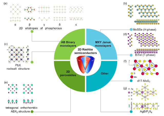
In this theoretical Perspective, we review SOC including the Rashba effect and Dresselhaus effect in 2D semiconductors. We start with an overview of the Hamiltonian model and characterization methods of the Rashba effect and Dresselhaus effect. Then, we summarize 2D SOC semiconductors, such as AB binary monolayers, Janus monolayers (especially for MXY Janus monolayers), 2D perovskites, and so forth. We also review manipulating methods of the Rashba effect, including external electric field, strain engineering, charge doping, interlayer interactions, proximity effect of substrates, and external magnetic field. Then, we briefly summarize the applications of SOC, including the generation, detection, and manipulation of spin currents in spin Hall effect transistors and spin field effect transistors. Finally, we provide an outlook on the SOC effect in low-dimensional semiconductors, including the nonlinear SOC Hamiltonian, 2D ferroelectric SOC semiconductors, and 1D SOC.

This theoretical Perspective reviews spin−orbit coupling (SOC), including the Rashba effect and Dresselhaus effect, in two-dimensional (2D) semiconductors. We first introduce the origin of the Rashba effect and Dresselhaus effect using the Hamiltonian models; we then summarize 2D Rashba semiconductors predicted by first-principles density functional theory (DFT) calculations, including AB binary monolayers, Janus monolayers, 2D perovskites, and so on. We also review various manipulating techniques of the Rashba effect on 2D semiconductors, such as external electric field, strain engineering, charge doping, interlayer interactions, proximity effect of substrates, and external magnetic field. We then briefly summarize the applications of SOC, including the generation, detection, and manipulation of spin currents in spin Hall effect transistors and spin field effect transistors.

Finally, we conclude this Perspective and propose three promising research fields of SOC in low-dimensional semiconductors, including the nonlinear SOC Hamiltonian model, 2D ferroelectric SOC semiconductors, and 1D Rashba model and semiconductors. This theoretical Perspective enriches the fundamental understanding of SOC in 2D semiconductors and will help in the design of new types of spintronic devices in future experiments.

practicalintroduction.com

Figure 2. (a) 3D band structure without SOC is 2-fold degenerate in spin. 3D band structures with (b) the Rashba effect and (c) Dresselhaus effect have band splitting and special spin textures. (d) 2D schematic illustration of the Rashba effect. ER represents the energy difference between the vertex of the energy curve and the degenerate energy at the high-symmetry point, and kR represents the corresponding momentum offset. Spin textures of (e) the Rashba effect and (f) Dresselhaus effect. Arrows indicate in-plane spin directions. Red (blue) represents the positive (negative) spin component along the y axis.

practicalintroduction.com

Figure 3. Schematic diagram of 2D Rashba semiconductors. (a) Top (upper row) and side (lower row) views of 2D binary phosphorene-type GeTe monolayers with α, β, γ, δ, and ϵ phases, where only the β-phase is suitable Rashba material. The green and brown balls represent two different atoms. Reprinted from ref 7. Copyright 2021 American Chemical Society. (b) Top (upper panel) and side (lower panel) views of H-phase MoSSe monolayer. Reprinted from ref 43. Copyright 2019 American Chemical Society. (c) (Left) top and (right) side views of square buckled PbX (X = S, Se, Te) monolayer. Blue and orange arrows denote vectors connecting Pb atom and its first- and second-nearest neighbors, respectively. Reprinted with permission from ref 8. Copyright 2017 American Physical Society. (d) Top (upper panel) and side (lower panel) views of T-phase BiTeI monolayer. Reprinted from ref 43. Copyright 2019 American Chemical Society. (e) Top (upper row) and side (lower row) views of 2D polar CsPbI3 structures from 3D tetragonal and orthorhombic bulk structures. The green, gray, and purple and balls represent Cs, Pb, and I atoms, respectively. 2D polar perovskites with ABX3 (A = Cs+, Rb+; B = Pb2+, Sn2+; X = Cl, Br, I) have similar structures. Reprinted from ref 16. Copyright 2021 American Chemical Society. (f) Structure of d1T-MoS2. Green arrows represent displacement vectors of the d1T phase with respect to the centrosymmetric 1T phase. Reprinted with permission from ref 44. Copyright 2014 American Physical Society. (g) Top (upper panel) and side (lower panel) views of ferroelectric AgBiP2X6 (X = S, Se, and Te) monolayer. Reprinted with permission from ref 17. Copyright 2020 American Physical Society.

practicalintroduciton.com

Figure 4. (a) Electric field dependence of the linear Rashba constants (αR) of the six MX2 (M = Mo, W; X, Y = S, Se, Te) monolayers. Reprinted from ref 12. Copyright 2017 American Physical Society. (b) Calculated Rashba constants (αKR) around the Γ point along the Γ-K direction under different biaxial in-plane strains for Janus MXY monolayers (M = Mo, W; X, Y = S, Se, Te; X ≠ Y). Reprinted with permission from ref 10. Copyright 2018 American Physical Society. (c) Calculated Rashba constants (αKR) around the Γ point along the Γ-K direction under the external electric field for Janus MXY monolayers (M = Mo, W; X, Y = S, Se, Te; X ≠ Y). Reprinted with permission from ref 10. Copyright 2018 American Physical Society. (d) Calculated Rashba constants (αR) under different uniaxial in-plane strains for AlBi monolayer. Reprinted from ref 7. Copyright 2021 American Chemical Society.

practicalintroduction.com

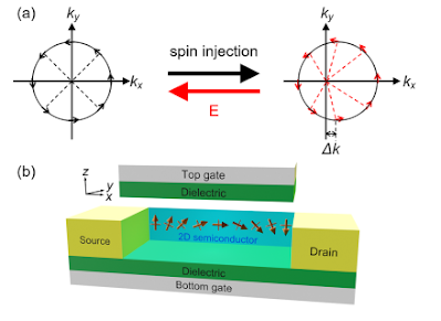
Figure 5. (a) Schematic illustration of the Rashba−Edelstein effect and inverse Rashba−Edelstein effect. In the Fermi contours with the Rashba effect, spins are perpendicular to the momentum. (Left to right, spin-tocharge conversion) When injecting the spin current polarized along the y direction, the charge current is generated by the spin texture shifts Δk along the x direction due to the spin-momentum locking injections. (Right to left, charge-to-spin conversion) When applying the electric field along the x direction, the Fermi surface is displaced by Δk and spins tilt, generating spin currents along the y direction. (b) A spin FET based on a 2D semiconductor.


Share:

Happy Wolrd Teacher Day

Daily Page View

Label

Adobe Acrobat Adobe Photoshop Alexa Rank Andorid Application Art Austria BUMN Beginner Belgium Blog Community Blogger Bupati Gresik CPNS/PPPK Canada Coin Market Cap Computers Cosmology Cryptocurrency Dancing Denmark Doctoral Doker Education Educational Excel Excel Table Features Film Finland French Gadget Gallery Garuda Emas Germany Google Analytics Google Form Hardware Homestay Hong Kong Ilovepdf Indrawan Vpp Interior Design Ireland Italy KKPR dan PKKPR Kampung hijau Karang Taruna Karir/Career Keyword Keywords LKPM LaTeX Linux Lowongan Kerja BUMN/SWASTA Mac Majalah Tech Material Physics Material Physics. Mechanical Engineering (ME) Microsoft 365 Microsoft Excel Microsoft Office Microsoft PowerPoint Microsoft Word NFC Nero Nero Burning 2021 Networking New Technology OSS RBA OTOMOTIF Operating Systems Optic PDF PT Aerotrans Services Indonesia (Garuda Indonesia Group) PT Astra Tol Nusantara (ASTRA Infra) PT Indomarco Prismatama (Indomaret Group) PT Indonesia Epson Industry PT Jakarta Industrial Estate Pulogadung PT Pertamina Training & Consulting (PTC) PT. Indofarma (Persero) PT. Kimia Farma Group Perizinan Berusaha Persetujuan Lingkungan Pinjaman Online Posgraduate Postgraduate PowerPoint Presentations Profil Perusahaan/Company Profil Profil-Perusahan Publisher Pyrolysis Quantum Computing Quantum Physics Quiz Renewable Energy Research SEO SWASTA Scholarship Semi conductor Semiconductor Sertifikat Halal Smartphone Spintronic Study Abroad Super Capasitor Superconductor Tata Cara Pendaftaran Surat Izin Usaha Industri (SIUI) Technology Tecnology Thailand The Best Trip & Travel Tutorial United Kingdom United Stated United States VGA card Website Windows 365 Windows Tips Word Document WordPress Zero Waste chromium tricks font iphone iphone 13 Pro iphone 13 Pro Max iphone 13 Pro Max gsmarena online zodiak